Hyperlens significantly boosts image resolution of microscopic objects
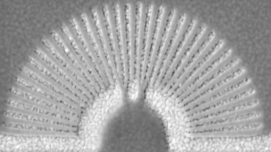
Scientists at the University of Buffalo have created a prototype visible light “hyperlens” that may help image objects that were once only clearly viewable through electron microscopes (Credit: University of Buffalo)
Using visible light magnified through a compound series of lenses to image small objects, standard optical microscopes have been with us for many centuries. Whilst continually being improved, the result of these many advances of optics and image-capturing techniques means that many high-end optical microscopes have now reached the limit of magnification possible as they push the resolution properties of light itself. In an attempt to resolve this issue, scientists at the University of Buffalo (UB) have created a prototype visible light “hyperlens” that may help image objects once only clearly viewable through electron microscopes.
The resolution limit for images captured by an optical microscope system is due to the diffraction of light from a viewed object. Put simply, as light passes through the circular aperture of a microscope lens, the light waves from very small points of light interfere with each other on the way through, causing the image to blur.
The diffraction problem is due to a phenomenon known as the “Rayleigh criterion”, which specifies the minimum separation distance between two observed objects that can be resolved into distinct objects. As the size of the aperture used in relation to the wavelength of light is inherent in the criterion’s formula, then the smaller the aperture and the closer in size an object is to the wavelength of light itself, the greater the diffraction and the more the image is blurred.
UB researchers working on metamaterials – that is, artificial materials engineered with properties not yet found in nature – claim to have overcome this diffraction limit problem by creating a photonic hyperlens that they say changes evanescent waves of light into propagating waves. In other words, they use these lenses to alter the properties of light from that which loses intensity rapidly (evanescent waves) to those that are increased in intensity (propagating waves).
The metamaterial hyperlenses first developed were made of silver and a dielectric insulating material arranged in concentric rings. Whilst this type of hyperlens worked very well at specific wavelengths of light, it suffered from large losses at resonant frequencies.
To help improve on this, UB researchers arranged minute slices of gold and PMMA (a clear thermoplastic) into a radiating semi-circular shape that the researchers point out looks like a very tiny Slinky suspended in its movement. This new shape turned out to be a much improved one, as it effectively ameliorates the diffraction limit on objects viewed in the visible light range.
An immediate use for such a device, the team believes, is that it could be combined with an optical waveguide to produce a hyperlens-based medical endoscope. As even high-resolution endoscopes can only resolve images of objects around 10,000 nanometers in size, a hyperlens-equipped endoscope could potentially increase that resolution to at least 250 nanometers or more, and may provide medical practitioners with that ability to locate tiny, hard-to-find cancers that could help catch the disease before it has time to spread.
“There is a great need in healthcare, nanotechnology and other areas to improve our ability to see tiny objects that elude even the most powerful optical systems,” said Natalia Litchinitser, PhD, professor of electrical engineering at UB. “The hyperlens we are developing is, potentially, a giant step toward solving this problem.”
The researchers also believe that the hyperlens may even eventually be capable of imaging single molecules in visible light, which has enormous implications for research in many fields, particularly chemistry and biology. In the field of physics, such a lens may also help such things as optical nanolithography, where light is shone through a mask to create a pattern on polymer or graphene films for integrated circuits, along with developments in the next generation of optoelectronic electronics, including sensors and data storage drives.
References: http://www.gizmag.com