New nanogenerator might set energy-generating car wheels in motion

nanogenerator-rolling-tires

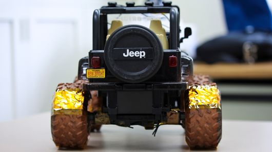
Xudong Wang’s team has developed a new way to harvest energy from rolling tires. The researchers used toy cars during the initial trials

Cars are one of mankind’s most revolutionary creations. But just like with the iPhone, space travel or Wi-Fi, there’s always room for improvement. In the eyes of a team of University of Wisconsin-Madison engineers, one of the more promising ways automotive technology might be improved upon lies in the energy wastage caused by friction as tires roll across the road. Armed with special nanogenerator and a toy Jeep, the researchers have demonstrated that this power can be captured and turned into electricity, a development that could bring about better fuel efficiency in the full-sized cars of the future.

According to Xudong Wang, associate professor of materials science and engineering at the University of Wisconsin, the friction created as a car’s tires run over the ground accounts for approximately 10 percent of the vehicle’s fuel usage. For him and PhD student Yanchao Mao, this presents a big opportunity to improve efficiency, so for the last year or so they have been building a device to tackle the problem.

nanogenerator-rolling-tires-2

Their work looks to harness the electrical charge that is created when certain materials come into contact with one another, much like what happens when you run a comb through your hair. This is known as the triboelectric effect and has been used in the early-stage development of promising technologies like electricity-generating touchscreens and clothing.

Not to be confused with the approach taken by Goodyear, which in March unveiled a concept tire that turns heat and motion into electricity using a fishnet pattern of thermo/piezoelectric material, Wang’s solution sees an electrode built into a section of the tire. As the wheel spins and this part of the tire comes into contact with the ground, the charge created by the friction causes electrons to move, in turn generating electricity.

To bring this new source of electricity to life, the team equipped the toy Jeep with LED lights. As the car moved forward, enough power was created to cause the lights to flash on and off, suggesting that this hitherto wasted energy could actually be captured and put to use.

Interestingly, the researchers also found that the amount of energy the system was able to produce was proportionate to both the weight of the vehicle and the speed at which it was traveling. Wang estimates that the solution could offer approximately a 10 percent increase in the average vehicle’s gas mileage.

References:http://www.gizmag.com/

Graphene takes on a new dimension

3d-graphene

A new process for creating 3D objects out of graphene opens up the possibility of fashioning a whole new range of innovative electronic devices

Graphene is the modern go-to material for scientists and engineers looking to create all manner of new electronic devices. From ultra-frugal light bulbs (both big and small), to super-efficient solar cells, flexible displays and much more, graphene is a multi-tasking marvel. However, in all of these instances, graphene in its original form of atom-thin, flat sheets has had to be used with peripheral supports and structures because it lacks a solid shape and form of its own. Now researchers from the University of Illinois at Urbana-Champaign (UIUC) have come up with a way of creating 3D objects out of graphene that opens up the possibility of fashioning a whole new range of innovative electronic devices.

To create 3D shapes in graphene, the researchers first had to ensure that their approach was sufficient to maintain the structural integrity of the material when it was subjected to deformation. As such, the team used an underlying substrate former over which they laid a film of graphene that had been soaked in solvent to make it swell and become malleable. Once overlaid on the former, the solvent then evaporated over time, leaving behind a layer of graphene that had taken on the shape of the underlying structure. In this way the team was able to produce a range of relatively intricate shapes.

3d-graphene-1

“To the best of our knowledge, this study is the first to demonstrate graphene integration to a variety of different microstructured geometries, including pyramids, pillars, domes, inverted pyramids, and the 3D integration of gold nanoparticles (AuNPs)/graphene hybrid structures,” said SungWoo Nam, assistant professor of mechanical science and engineering at UIUC. “Our swelling, shrinking, and adaptation steps are optimized to minimize the degree of graphene suspension around the 3D microstructures and facilitate successful 3D integration. We control the amount of substrate swelling by adjusting the time of immersion in organic solvent and the mixing ratios of monomer and curing agent of the polydimethylsiloxane (PDMS) substrate.”

Varying in size from just 3.5 to 50 μm, the dimensions of the graphene microstructures developed by UIUC put them right in the middle of a range of electronic devices, including various types of photodetectors, nano antennas, and other sub-miniature components that were once only the domain of silicon-based products. According to the team, these factors, along with graphene’s high carrier mobility, chemical inertness, and biocompatibility, mean that three-dimensional graphene could be adapted over even wider areas.

“We also expect that our new 3D integration approach will facilitate advanced classes of hybrid devices between microelectromechanical systems (MEMS) and 2D materials for sensing and actuation,” said SungWoo Nam.

Due to the fragility of atom-thin graphene, previous methods to bend or mold it into complex shapes resulted in uneven, ill-formed objects at best, and a ruptured mess at worst. In investigating the new technique, the researchers at UIUC were diligent in their testing of the formed graphene via electron microscopy, atomic force microscopy, Raman spectroscopy, and electrical resistance measurement to confirm that it maintained its shape and consistency after forming.

“Our results demonstrate a simple, versatile, and scalable method to integrate graphene with 3D geometries with various morphologies and dimensions,” said Jonghyun Choi, a graduate student in Nam’s research group. “Not only are these 3D features larger than those reported in previous works, but we also demonstrate the uniformity and damage-free nature of integrated graphene around the 3D features.”

References:http://www.gizmag.com/

Compound discovery sets stage for speedier electronic devices

niobium-phosphide-large-magnetoresistance-electronics

lectronics can get faster and better more quickly thanks to the discovery that niobium phosphide has an especially high magnetoresistance – a phenomenon illustrated here in which electrons are deflected from their original direction of flow (green arrow) by a magnetic field (black arrows), increasing electric resistance

A discovery at the Max Planck Institute for Chemical Physics of Solids could pave the way for further leaps forward in the speed of electronic systems. The scientists, who worked in collaboration with colleagues at Helmholtz-Zentrum Dresden-Rossendorf and Radbound University, found that a material called niobium phosphide, which is a compound of transition metal niobium and phosphorus, dramatically increases its resistance in a magnetic field. The material could find use in faster, higher-capacity hard drives and other electronic components.

Electronic components such as hard disks typically use layers of different materials in filigree structure (tiny beads and threads of metal soldered onto the surface) to exploit a phenomenon known as magnetoresistance to develop a high electric resistance, which allows for higher density of data and thus greater storage capacity.

What happens here is that a tiny amount of electricity causes the charge carriers to deflect via a phenomenon called the Lorentz force, and then that causes electrons to flow in the “wrong” direction – thereby increasing electric resistance and allowing a very precise read of the data that’s magnetically stored in a given location.

“The faster the electrons in the material move, the greater the Lorentz force and thus the effect of a magnetic field,” explains study lead author Binghai Yan. The electrons in this material, niobium phosphide, travel very quickly. Niobium phosphide contains superfast charge carriers, or relativistic electrons, that move at 300 km/s (186 mi/s), which is one-thousandth the speed of light. And that extreme speed allows the resistance to increase by a factor of 10,000.

The researchers believe that niobium phosphide has “enormous potential for future applications in information technology” – not only in hard drives but also in many other electronic components that use magnetoresistance to function.

References:http://www.gizmag.com/

Solar-powered hydrogen generation using two of the most abundant elements on Earth

hematite-hydrogen

By smoothing the surface of hematite, a team of researchers achieved “unassisted” water splitting using the abundant rust-like mineral hermatite and silicon to capture and store solar energy within hydrogen gas

One potential clean energy future requires an economical, efficient, and relatively simple way to generate copious amounts of hydrogen for use in fuel-cells and hydrogen-powered vehicles. Often achieved by using electricity to split water molecules into hydrogen and oxygen, the ideal method would be to mine hydrogen from water using electricity generated directly from sunlight without the addition of any external power source. Hematite – the mineral form of iron – used in conjunction with silicon has shown some promise in this area, but low conversion efficiencies have slowed research. Now scientists have discovered a way to make great improvements, giving hope to using two of the most abundant elements on earth to efficiently produce hydrogen.

Hematite holds potential for use in low-power photoelectrochemical water splitting (where energy, in the form of light, is the input and chemical energy is the output) to release hydrogen due to its low turn-on voltage of less than 0.3 volts when exposed to sunlight. Unfortunately, that voltage is too low to initiate water-splitting so a number of improvements to the surface of hematite have been sought to improve current flow.

In this vein, researchers from Boston College, UC Berkeley, and China’s University of Science and Technology have hit upon the technique of “re-growing” the hematite, so that a smoother surface is obtained along with a higher energy yield. In fact, this new version has doubled the electrical output, and moved one step closer to enabling practical, large-scale energy-harvesting and hydrogen generation.

“By simply smoothing the surface characteristics of hematite, this close cousin of rust can be improved to couple with silicon, which is derived from sand, to achieve complete water splitting for solar hydrogen generation,” said Boston College associate professor of chemistry Dunwei Wang. “This unassisted water splitting, which is very rare, does not require expensive or scarce resources.”

Working on previous work that realized gains in the photoelectrochemical turn-on voltage from the use of smooth surface coatings, the team re-assessed the hematite surface structure by employing a synchrotron particle accelerator at the Lawrence Berkeley National Laboratory. Concentrating on massaging the hematite’s surface deficiencies to see if this would result in improvements, the researchers used physical vapor deposition to layer hematite onto a borosilicate glass substrate and create a photoanode. They then baked the devices to produce a thin, even film of iron oxide across their surfaces.

Subsequent tests of this new amalgam resulted in an immediate improvement in turn-on voltage, and a substantial increase in photovoltage from 0.24 volts to 0.80 volts. Whilst this new hydrogen harvesting process only realized an efficiency of 0.91 percent, it is the very first time that the combination of hematite and amorphous silicon has been shown to produce any meaningful efficiencies of conversion at all.

As a result, this research has shown that progress has been made towards the possibility of producing photoelectrochemical energy harvesting that is totally self-sufficient, uses abundantly available materials, and is easy to produce.

“This offers new hope that efficient and inexpensive solar fuel production by readily available natural resources is within reach,” said Wang. “Getting there will contribute to a sustainable future powered by renewable energy.”

References:http://www.gizmag.com/