Nano memory cell can mimic the brain’s long-term memory

150512075107_1_540x360

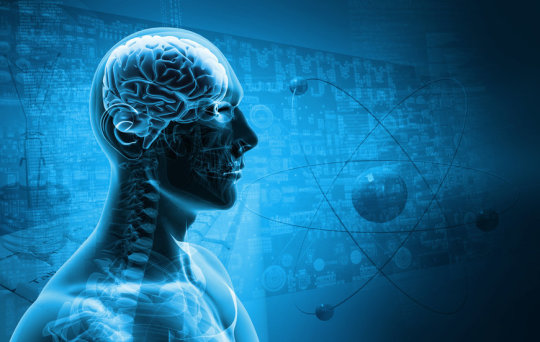
RMIT University researchers have mimicked the way the human brain processes information with the development of an electronic long-term memory cell.

Researchers at the MicroNano Research Facility (MNRF) have built the one of the world’s first electronic multi-state memory cell which mirrors the brain’s ability to simultaneously process and store multiple strands of information.

The development brings them closer to imitating key electronic aspects of the human brain — a vital step towards creating a bionic brain — which could help unlock successful treatments for common neurological conditions such as Alzheimer’s and Parkinson’s diseases.

The discovery was recently published in the materials science journalAdvanced Functional Materials.

Project leader Dr Sharath Sriram, co-leader of the RMIT Functional Materials and Microsystems Research Group, said the ground-breaking development imitates the way the brain uses long-term memory.

“This is the closest we have come to creating a brain-like system with memory that learns and stores analog information and is quick at retrieving this stored information,” Dr Sharath said.

“The human brain is an extremely complex analog computer… its evolution is based on its previous experiences, and up until now this functionality has not been able to be adequately reproduced with digital technology.”

The ability to create highly dense and ultra-fast analog memory cells paves the way for imitating highly sophisticated biological neural networks, he said.

The research builds on RMIT’s previous discovery where ultra-fast nano-scale memories were developed using a functional oxide material in the form of an ultra-thin film — 10,000 times thinner than a human hair.

Dr Hussein Nili, lead author of the study, said: “This new discovery is significant as it allows the multi-state cell to store and process information in the very same way that the brain does.

“Think of an old camera which could only take pictures in black and white. The same analogy applies here, rather than just black and white memories we now have memories in full color with shade, light and texture, it is a major step.”

While these new devices are able to store much more information than conventional digital memories (which store just 0s and 1s), it is their brain-like ability to remember and retain previous information that is exciting.

“We have now introduced controlled faults or defects in the oxide material along with the addition of metallic atoms, which unleashes the full potential of the ‘memristive’ effect — where the memory element’s behaviour is dependent on its past experiences,” Dr Nili said.

Nano-scale memories are precursors to the storage components of the complex artificial intelligence network needed to develop a bionic brain.

Dr Nili said the research had myriad practical applications including the potential for scientists to replicate the human brain outside of the body — which would remove the ethical barriers involved in experimenting on humans.

“If you could replicate a brain outside the body, it would minimise ethical issues involved in treating and experimenting on the brain which can lead to better understanding of neurological conditions,” Dr Nili said.

The research, supported by the Australian Research Council, was conducted in collaboration with the University of California Santa Barbara.

 References:http://www.sciencedaily.com/

Mobile battery life can be prolonged with system settings

By using crowdsourced measurements researchers explain the energy impact of smartphone system settings, and their results show how to improve a mobile device’s battery lifetime by adjusting the settings.

The NODES research group from University of Helsinki, Finland, has studied how the impact of different settings on battery lifetime can be estimated using crowdsourced measurements from a large community of devices. The research article “Energy Modeling of System Settings: A Crowdsourced Approach” was published in the 13th IEEE International Conference on Pervasive Computing (PerCom) in St Louis, USA, on 24 March 2015.

Mobile devices have a large number of different adjustable system settings whose energy impact can be difficult to understand for the average user, and even for the expert.

Some system settings have a direct and significant correlation with energy consumption, for example screen brightness and network connectivity. The energy impact of system settings and their combinations, such as the combination of roaming, high operating temperature, and bad signal strength, are much more difficult to predict. The research article by the Finnish computer scientists demonstrates that the energy impact of these non­trivial system setting combinations can be significant, and presents a new learning based method for assessing this impact.

The effects of different settings need to be modelled as a whole

The research is based on a large dataset that consists of device usage data gathered from over 150,000 smartphones and tablets. The dataset covers real life daily usage patterns and together with laboratory based specific high precision measurements serves as the empirical basis for the research work.

The energy model for system settings proposed in the research study makes it possible to give personalized, practical energy recommendations to the smartphone user. The research findings include the following:

  • Wi­Fi signal strength dropping one bar can cause over 13% battery life loss
  • High temperature can cause even 50% battery life loss, and high temperature is not always related to high CPU load
  • Automatic screen brightness is in most cases better than the manual setting

In addition to CPU, battery temperature and distance traveled together offer a good predictor of battery lifetime.

References: http://www.sciencedaily.com/

New device could greatly improve speech and image recognition

150511172759_1_540x360

Clockwise, photo of the prototype device; schematic of the eight-terminal magnonic holographic memory prototype; collection of experimental data obtained for two magnonic matrixes.

Researchers at the University of California, Riverside Bourns College of Engineering and the Russian Academy of Sciences have successfully demonstrated pattern recognition using a magnonic holographic memory device, a development that could greatly improve speech and image recognition hardware.

Pattern recognition focuses on finding patterns and regularities in data. The uniqueness of the demonstrated work is that the input patterns are encoded into the phases of the input spin waves.

Spin waves are collective oscillations of spins in magnetic materials. Spin wave devices are advantageous over their optical counterparts because they are more scalable due to a shorter wavelength. Also, spin wave devices are compatible with conventional electronic devices and can be integrated within a chip.

The researchers built a prototype eight-terminal device consisting of a magnetic matrix with micro-antennas to excite and detect the spin waves. Experimental data they collected for several magnonic matrixes show unique output signatures correspond to specific phase patterns. The microantennas allow the researchers to generate and recognize any input phase pattern, a big advantage over existing practices.

Then spin waves propagate through the magnetic matrix and interfere. Some of the input phase patterns produce high output voltage, and other combinations results in a low output voltage, where “high” and “low” are defined regarding the reference voltage (i.e. output is high if the output voltage is higher than 1 millivolt, and low if the voltage is less than 1 millivolt.

It takes about 100 nanoseconds for recognition, which is the time required for spin waves to propagate and to create the interference pattern.

The most appealing property of this approach is that all of the input ports operate in parallel. It takes the same amount of time to recognize patterns (numbers) from 0 to 999, and from 0 to 10,000,000. Potentially, magnonic holographic devices can be fundamentally more efficient than conventional digital circuits.

The work builds upon findings published last year by the researchers, who showed a 2-bit magnonic holographic memory device can recognize the internal magnetic memory states via spin wave superposition. That work was recognized as a top 10 physics breakthrough by Physics World magazine.

“We were excited by that recognition, but the latest research takes this to a new level,” said Alex Khitun, a research professor at UC Riverside, who is the lead researcher on the project. “Now, the device works not only as a memory but also a logic element.”

The latest findings were published in a paper called “Pattern recognition with magnonic holographic memory device” in the journal Applied Physics Letters. In addition to Khitun, authors are Frederick Gertz, a graduate student who works with Khitun at UC Riverside, and A. Kozhevnikov, Y. Filimonov and G. Dudko, all from the Russian Academy of Sciences.

Holography is a technique based on the wave nature of light which allows the use of wave interference between the object beam and the coherent background. It is commonly associated with images being made from light, such as on driver’s licenses or paper currency. However, this is only a narrow field of holography.

Holography has been also recognized as a future data storing technology with unprecedented data storage capacity and ability to write and read a large number of data in a highly parallel manner.

The main challenge associated with magnonic holographic memory is the scaling of the operational wavelength, which requires the development of sub-micrometer scale elements for spin wave generation and detection.

References:http://www.sciencedaily.com/

Controlling light: Scientists tune light waves by pairing exotic 2-D materials

150520100607_1_540x360

Researchers have shown that a DC voltage applied to layers of graphene and boron nitride can be used to control light emission from a nearby atom. Here, graphene is represented by a maroon-colored top layer; boron nitride is represented by yellow-green lattices below the graphene; and the atom is represented by a grey circle. A low concentration of DC voltage (in blue) allows the light to propagate inside the boron nitride, forming a tightly confined waveguide for optical signals. Researchers have shown that a DC voltage applied to layers of graphene and boron nitride can be used to control light emission from a nearby atom. Here, graphene is represented by a maroon-colored top layer; boron nitride is represented by yellow-green lattices below the graphene; and the atom is represented by a grey circle. A low concentration of DC voltage (in blue) allows the light to propagate inside the boron nitride, forming a tightly confined waveguide for optical signals.

Researchers have found a way to couple the properties of different two-dimensional materials to provide an exceptional degree of control over light waves. They say this has the potential to lead to new kinds of light detection, thermal-management systems, and high-resolution imaging devices.

The new findings — using a layer of one-atom-thick graphene deposited on top of a similar 2-D layer of a material called hexagonal boron nitride (hBN) — are published in the journal Nano Letters. The work is co-authored by MIT associate professor of mechanical engineering Nicholas Fang and graduate student Anshuman Kumar, and their co-authors at IBM’s T.J. Watson Research Center, Hong Kong Polytechnic University, and the University of Minnesota.

Although the two materials are structurally similar — both composed of hexagonal arrays of atoms that form two-dimensional sheets — they each interact with light quite differently. But the researchers found that these interactions can be complementary, and can couple in ways that afford a great deal of control over the behavior of light.

The hybrid material blocks light when a particular voltage is applied to the graphene, while allowing a special kind of emission and propagation, called “hyperbolicity,” when a different voltage is applied — a phenomenon not seen before in optical systems, Fang says. One of the consequences of this unusual behavior is that an extremely thin sheet of material can interact strongly with light, allowing beams to be guided, funneled, and controlled by voltages applied to the sheet.

“This poses a new opportunity to send and receive light over a very confined space,” Fang says, and could lead to “unique optical material that has great potential for optical interconnects.” Many researchers see improved interconnection of optical and electronic components as a path to more efficient computation and imaging systems.

Light’s interaction with graphene produces particles called plasmons, while light interacting with hBN produces phonons. Fang and his colleagues found that when the materials are combined in a certain way, the plasmons and phonons can couple, producing a strong resonance.

The properties of the graphene allow precise control over light, while hBN provides very strong confinement and guidance of the light. Combining the two makes it possible to create new “metamaterials” that marry the advantages of both, the researchers say.

Phaedon Avouris, a researcher at IBM and co-author of the paper, says, “The combination of these two materials provides a unique system that allows the manipulation of optical processes.”

The combined materials create a tuned system that can be adjusted to allow light only of certain specific wavelengths or directions to propagate, they say. “We can start to selectively pick some frequencies [to let through], and reject some,” Kumar says.

These properties should make it possible, Fang says, to create tiny optical waveguides, about 20 nanometers in size — the same size range as the smallest features that can now be produced in microchips. This could lead to chips that combine optical and electronic components in a single device, with far lower losses than when such devices are made separately and then interconnected, they say.

Co-author Tony Low, a researcher at IBM and the University of Minnesota, says, “Our work paves the way for using 2-D material heterostructures for engineering new optical properties on demand.”

Another potential application, Fang says, comes from the ability to switch a light beam on and off at the material’s surface; because the material naturally works at near-infrared wavelengths, this could enable new avenues for infrared spectroscopy, he says. “It could even enable single-molecule resolution,” Fang says, of biomolecules placed on the hybrid material’s surface.

Sheng Shen, an assistant professor of mechanical engineering at Carnegie Mellon University who was not involved in this research, says, “This work represents significant progress on understanding tunable interactions of light in graphene-hBN.” The work is “pretty critical” for providing the understanding needed to develop optoelectronic or photonic devices based on graphene and hBN, he says, and “could provide direct theoretical guidance on designing such types of devices. … I am personally very excited about this novel theoretical work.”

The research team also included Kin Hung Fung of Hong Kong Polytechnic University. The work was supported by the National Science Foundation and the Air Force Office of Scientific Research.

References:http://www.sciencedaily.com/