The Future of Your PC’s Hardware

152683-2612p088-2b

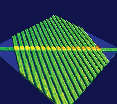
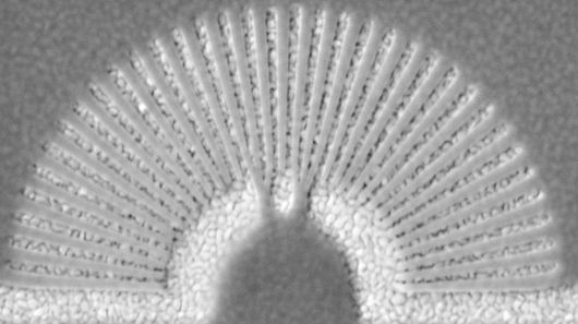
Since the dawn of electronics, we’ve had only three types of circuit components–resistors, inductors, and capacitors. But in 1971, UC Berkeley researcher Leon Chua theorized the possibility of a fourth type of component, one that would be able to measure the flow of electric current: the memristor. Now, just 37 years later, Hewlett-Packard has built one
What is it? As its name implies, the memristor can “remember” how much current has passed through it. And by alternating the amount of current that passes through it, a memristor can also become a one-element circuit component with unique properties. Most notably, it can save its electronic state even when the current is turned off, making it a great candidate to replace today’s flash memory.

Memristors will theoretically be cheaper and far faster than flash memory, and allow far greater memory densities. They could also replace RAM chips as we know them, so that, after you turn off your computer, it will remember exactly what it was doing when you turn it back on, and return to work instantly. This lowering of cost and consolidating of components may lead to affordable, solid-state computers that fit in your pocket and run many times faster than today’s PCs.

Someday the memristor could spawn a whole new type of computer, thanks to its ability to remember a range of electrical states rather than the simplistic “on” and “off” states that today’s digital processors recognize. By working with a dynamic range of data states in an analog mode, memristor-based computers could be capable of far more complex tasks than just shuttling ones and zeroes around.

When is it coming? Researchers say that no real barrier prevents implementing the memristor in circuitry immediately. But it’s up to the business side to push products through to commercial reality. Memristors made to replace flash memory (at a lower cost and lower power consumption) will likely appear first; HP’s goal is to offer them by 2012. Beyond that, memristors will likely replace both DRAM and hard disks in the 2014-to-2016 time frame. As for memristor-based analog computers, that step may take 20-plus years.

32-Core CPUs From Intel and AMD

152683-2612p088-3b

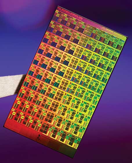
If your CPU has only a single core, it’s officially a dinosaur. In fact, quad-core computing is now commonplace; you can even get laptop computers with four cores today. But we’re really just at the beginning of the core wars: Leadership in the CPU market will soon be decided by who has the most cores, not who has the fastest clock speed.
What is it? With the gigahertz race largely abandoned, both AMD and Intel are trying to pack more cores onto a die in order to continue to improve processing power and aid with multitasking operations. Miniaturizing chips further will be key to fitting these cores and other components into a limited space. Intel will roll out 32-nanometer processors (down from today’s 45nm chips) in 2009.

When is it coming? Intel has been very good about sticking to its road map. A six-core CPU based on the Itanium design should be out imminently, when Intel then shifts focus to a brand-new architecture called Nehalem, to be marketed as Core i7. Core i7 will feature up to eight cores, with eight-core systems available in 2009 or 2010. (And an eight-core AMD project called Montreal is reportedly on tap for 2009.)

After that, the timeline gets fuzzy. Intel reportedly canceled a 32-core project called Keifer, slated for 2010, possibly because of its complexity (the company won’t confirm this, though). That many cores requires a new way of dealing with memory; apparently you can’t have 32 brains pulling out of one central pool of RAM. But we still expect cores to proliferate when the kinks are ironed out: 16 cores by 2011 or 2012 is plausible (when transistors are predicted to drop again in size to 22nm), with 32 cores by 2013 or 2014 easily within reach. Intel says “hundreds” of cores may come even farther down the line.

References: http://www.pcworld.com

Hyperlens significantly boosts image resolution of microscopic objects

hyperlens

Scientists at the University of Buffalo have created a prototype visible light “hyperlens” that may help image objects that were once only clearly viewable through electron microscopes (Credit: University of Buffalo)

Using visible light magnified through a compound series of lenses to image small objects, standard optical microscopes have been with us for many centuries. Whilst continually being improved, the result of these many advances of optics and image-capturing techniques means that many high-end optical microscopes have now reached the limit of magnification possible as they push the resolution properties of light itself. In an attempt to resolve this issue, scientists at the University of Buffalo (UB) have created a prototype visible light “hyperlens” that may help image objects once only clearly viewable through electron microscopes.

The resolution limit for images captured by an optical microscope system is due to the diffraction of light from a viewed object. Put simply, as light passes through the circular aperture of a microscope lens, the light waves from very small points of light interfere with each other on the way through, causing the image to blur.

The diffraction problem is due to a phenomenon known as the “Rayleigh criterion”, which specifies the minimum separation distance between two observed objects that can be resolved into distinct objects. As the size of the aperture used in relation to the wavelength of light is inherent in the criterion’s formula, then the smaller the aperture and the closer in size an object is to the wavelength of light itself, the greater the diffraction and the more the image is blurred.

UB researchers working on metamaterials – that is, artificial materials engineered with properties not yet found in nature – claim to have overcome this diffraction limit problem by creating a photonic hyperlens that they say changes evanescent waves of light into propagating waves. In other words, they use these lenses to alter the properties of light from that which loses intensity rapidly (evanescent waves) to those that are increased in intensity (propagating waves).

The metamaterial hyperlenses first developed were made of silver and a dielectric insulating material arranged in concentric rings. Whilst this type of hyperlens worked very well at specific wavelengths of light, it suffered from large losses at resonant frequencies.

To help improve on this, UB researchers arranged minute slices of gold and PMMA (a clear thermoplastic) into a radiating semi-circular shape that the researchers point out looks like a very tiny Slinky suspended in its movement. This new shape turned out to be a much improved one, as it effectively ameliorates the diffraction limit on objects viewed in the visible light range.

An immediate use for such a device, the team believes, is that it could be combined with an optical waveguide to produce a hyperlens-based medical endoscope. As even high-resolution endoscopes can only resolve images of objects around 10,000 nanometers in size, a hyperlens-equipped endoscope could potentially increase that resolution to at least 250 nanometers or more, and may provide medical practitioners with that ability to locate tiny, hard-to-find cancers that could help catch the disease before it has time to spread.

“There is a great need in healthcare, nanotechnology and other areas to improve our ability to see tiny objects that elude even the most powerful optical systems,” said Natalia Litchinitser, PhD, professor of electrical engineering at UB. “The hyperlens we are developing is, potentially, a giant step toward solving this problem.”

The researchers also believe that the hyperlens may even eventually be capable of imaging single molecules in visible light, which has enormous implications for research in many fields, particularly chemistry and biology. In the field of physics, such a lens may also help such things as optical nanolithography, where light is shone through a mask to create a pattern on polymer or graphene films for integrated circuits, along with developments in the next generation of optoelectronic electronics, including sensors and data storage drives.

References: http://www.gizmag.com

Team presents induction-powered biosensor chips detecting many molecules in vivo

achipplacedu

It’s only a centimeter long, it’s placed under your skin, it’s powered by a patch on the surface of your skin and it communicates with your mobile phone. The new biosensor chip developed at EPFL is capable of simultaneously monitoring the concentration of a number of molecules, such as glucose and cholesterol, and certain drugs.

The future of medicine lies in ever greater precision, not only when it comes to diagnosis but also drug dosage. The blood work that medical staff rely on is generally a snapshot indicative of the moment the blood is drawn before it undergoes hours – or even days – of analysis.
Several EPFL laboratories are working on devices allowing constant analysis over as long a period as possible. The latest development is the biosensor chip, created by researchers in the Integrated Systems Laboratory working together with the Radio Frequency Integrated Circuit Group. Sandro Carrara is unveiling it today at the International Symposium on Circuits and Systems (ISCAS) in Lisbon.

Autonomous operation

“This is the world’s first chip capable of measuring not just pH and temperature, but also metabolism-related molecules like glucose, lactate and cholesterol, as well as drugs,” said Dr Carrara. A group of electrochemical sensors works with or without enzymes, which means the device can react to a wide range of compounds, and it can do so for several days or even weeks.
This one-centimetre square device contains three main components: a circuit with six sensors, a control unit that analyses incoming signals, and a radio transmission module. It also has an induction coil that draws power from an external battery attached to the skin by a patch. “A simple plaster holds together the battery, the coil and a Bluetooth module used to send the results immediately to a mobile phone,” said Dr Carrara.

1-achipplacedu

Contactless, in vivo monitoring

The chip was successfully tested in vivo on mice at the Institute for Research in Biomedicine (IRB) in Bellinzona, where researchers were able to constantly monitor glucose and paracetamol levels without a wire tracker getting in the way of the animals’ daily activities. The results were extremely promising, which means that clinical tests on humans could take place in three to five years – especially since the procedure is only minimally invasive, with the chip being implanted just under the epidermis.
“Knowing the precise and real-time effect of drugs on the metabolism is one of the keys to the type of personalised, precision medicine that we are striving for,” said Dr Carrara.

References: http://phys.org

Researchers develop two-legged robot that walks like an animated character

70-researchersd

When Walt Disney created Mickey Mouse, he didn’t give much thought to how he might bring his character to life in the real world. But robotics now puts that possibility within reach, so Disney researchers have found a way for a robot to mimic an animated character’s walk.

Beginning with an animation of a diminutive, peanut-shaped character that walks with a rolling, somewhat bow-legged gait, Katsu Yamane and his team at Disney Research Pittsburgh analyzed the character’s motion to design a robotic frame that could duplicate the walking motion using 3D-printed links and servo motors, while also fitting inside the character’s skin. They then created control software that could keep the robot balanced while duplicating the character’s gait as closely as possible.
“The biggest challenge is that designers don’t necessarily consider physics when they create an animated character,” said Yamane, senior research scientist. Roboticists, however, wrestle with physical constraints throughout the process of creating a real-life version of the character.
“It’s important that, despite physical limitations, we do not sacrifice style or the quality of motion,” Yamane said. The robots will need to not only look like the characters, but move in the way people are accustomed to seeing those characters move.
Yamane and Joohyung Kim of Disney Research Pittsburgh and Seungmoon Song, a Ph.D. student at Carnegie Mellon University’s Robotics Institute, focused first on developing the lower half of such a robot.
“Walking is where physics matter the most,” Yamane explained. “If we can find a way to make the lower half work, we can use the exact same procedure for the upper body.”
They will describe the techniques and technologies they used to create the bipedal robot at the IEEE International Conference on Robotics and Automation, ICRA 2015, May 26-30 in Seattle.
Compromises were inevitable. For instance, an analysis of the animated character showed that its ankle and foot had three joints, each of which had three degrees of freedom. Integrating nine actuators in a foot isn’t practical. And the researchers realized that the walking motion in the animation wasn’t physically realizable – if the walking motion in the animation was used on a real robot, the robot would fall down.
By studying the dynamics of the walking motion in simulation, the researchers realized they could mimic the motion by building a leg with a hip joint that has three degrees of freedom, a knee joint with a single degree of freedom and an ankle with two degrees of freedom.
Because the joints of the robot differ from what the analysis showed that the animated character had, the researchers couldn’t duplicate the character’s joint movements, but identified the position trajectories of the character’s pelvis, hips, knees, ankle and toes that the robot would need to duplicate. To keep the robot from falling, the researchers altered the motion, such as by keeping the character’s stance foot flat on the ground.
They then optimized the trajectories to minimize any deviation from the target motions, while ensuring that the robot was stable.

References: http://phys.org